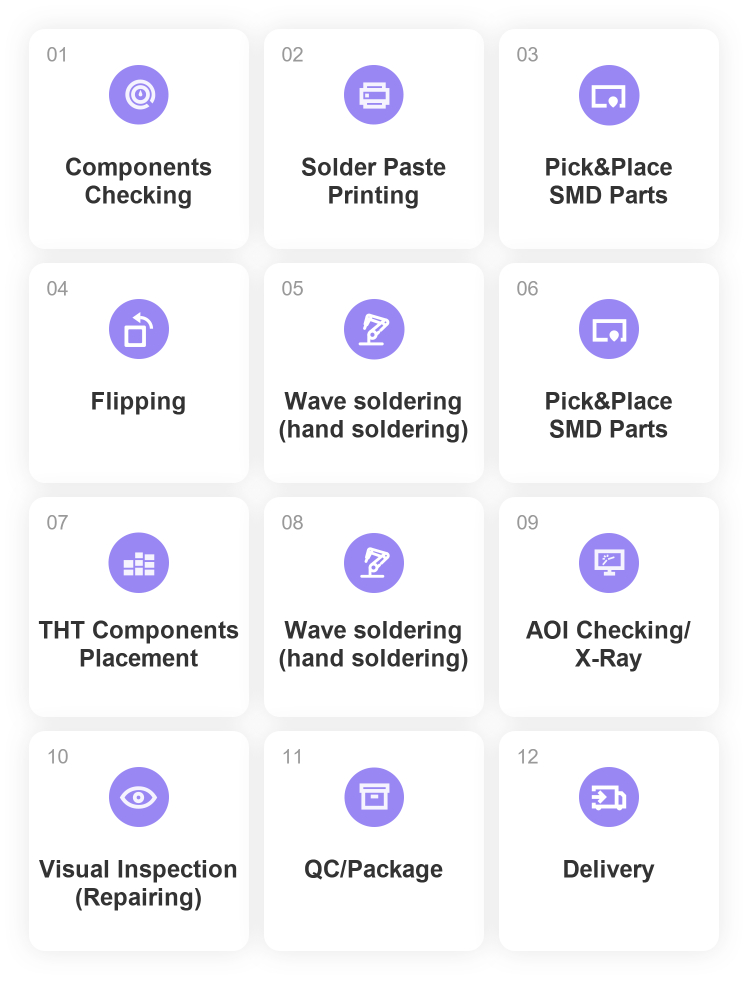
NextPCB provides efficient and high-quality turnkey PCB assembly service to its customer. In order to achieve the fastest possible turnaround of the highest quality product, we continuously strive to improve our services and to make each step as efficient as possible. One of the most important factors in the overall efficiency of each PCB assembly project is the client’s understanding of PCB assembly process.
This page provides an overview of some standard but important turnkey PCB assembly process. This is a brief overview only, if you are more interested in, welcome to our factory.Incoming Material Inspection
An incoming inspection, also known as a receiving inspection or material inspection, validates the quality of purchased raw materials based on set acceptance criteria. It is performed by quality assurance personnel in the manufacturing facility to resolve quality issues during pre-production. Incoming inspection results follow an identification tagging system to determine required actions when an item is tagged as accepted, conditionally accepted, or rejected.
NextPCB team will do full check on incoming material inspection to control the assembly quality. Components counting, package confirm, quantity confirm are in this process.
SMT Solder Paste Printing
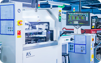
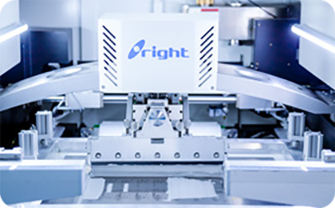
Solder paste (or solder cream) is a material used in the manufacture of printed circuit boards to connect surface mount components to pads on the board. Before soldering, all PCB boards should print solder paste so that the components can be soldered by pick & place machine.
Pick & Place Assembly
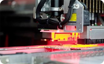
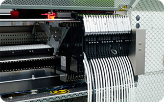
Once bare PCBs printed solder paste, they are moved to NextPCB’s automated Pick & Place machines for the actual mounting of components on their associated pads. Part placement is 100% machine automated for maximum accuracy and efficiency, and uses the project’s Centroid file for component coordinates and rotation data. The boards are again inspected after components have been mounted to ensure all placements are accurate before the soldering process begins.This stage might need to be performed multiple times, depending upon the specifics of a given project. Double-sided SMT boards require one round of placement for the top and one for the bottom, and projects requiring wave soldering due to a high number of through-hole parts will normally have their components machine-placed as well.
Reflow Soldering
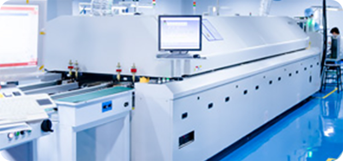
With parts mounted securely in place with solder paste underneath their pads, it is time for the PCBs to enter the reflow soldering oven. This is the most common method for PCB assembly in the industry today since it is much more flexible in terms of PCB layout requirements compared with wave or hand soldering. Most of the time, NextPCB can use reflow soldering for a majority of the parts on a board, and then pass the mostly-assembled boards to our highly skilled hand soldering team for the final few connectors and through hole components. NextPCB has more than 6 reflow oven in its plant.
For double-sided assembly projects, the boards will need to be reflowed once for each side. A special adhesive is applied underneath the components that were soldered in the first run to prevent them from detaching and falling off the board when their solder is re-heated.
AOI Checking
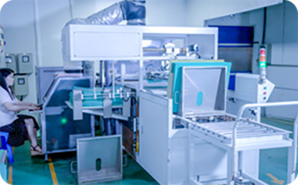
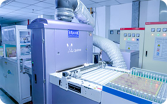
After Reflow oven soldering, NextPCB will put the assembly board to a machine which is automatic optical inspection machine to check quality for pick and place components. This process is checking that the pin connected with pads is correct or not, the tin on the pads is over or not, etc.
X-Ray Inspection
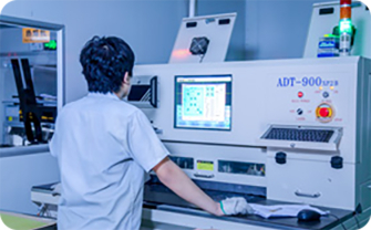
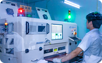
After a reflow oven process, any boards including BGA, QFN, or other lead-less package types are sent for X-Ray Inspection; this service is included by default on all NextPCB quotations which include such parts.
Wave Soldering
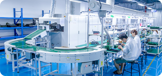
Quality for Every Stage of PCB and assembly in NextPCB has been controlled. In PCB assembly process, it has Initial Sample Inspection,
Defective Analysis, Functional Repairing, etc to control your PCBA projects to be high quality.