1 oz Copper PCB - NextPCB
Introduction to 1 Oz Copper Printed Circuit Boards
1 oz copper PCB is the standard thickness of copper printed circuit boards during manufacturing and assembly Processes. Suppose an ounce is not a standard unit in your location, 1 oz is equivalent to 1.38 mils (1.38 thousandths of an inch).
The PCB industry is growing in numbers daily as it offers a wide range of applications in several global industries. As such, there is a need for PCB manufacturers to follow PCB design standards, ensuring they fabricate and manufacture the best PCBs.
Copper is an integral material in the PCB design process in PCB manufacturing. It offers unique electrical and thermal characteristics necessary for signal transmission than any known metal. Copper actively dissipates heat away from essential circuit board components.
The use of copper has electrical advantages. When an electrical current is made to flow through metals, it is in direct conflict with resistivity. All materials offer a degree of resistance to current flow. Hence, a material with low resistivity has more electrical conductivity.
Copper is especially incredible in distributing electricity to homes and industries. Transmission and distribution lines often supply immense electrical power at a time to locations. However, unlike copper, many metals cannot handle intensive power loads as they could melt.
Keeping these details in mind has spurred PCB manufacturers to consider using 1 oz copper PCB in many electronic applications.
Selecting the Right 1 oz Copper PCB Thickness
Remember that increasing your copper thickness beyond 1 ounce (1.37 mils) will increase your PCB cost linearly. While some applications require thicker copper PCBs for their intended applications, fabricating and manufacturing such PCBs are expensive and time-consuming.
Also, when designing your circuit board, it is essential to know the required thickness, which could provide the necessary space between copper features. There is a general guideline for minimum spacing based on copper weight. Take a look.
| Copper PCB weight | Min. Recommended Space between Copper Features |
|---|---|
| 1 oz | 3.5 mil (0.089 mm) |
| 2 oz | 8 mil (0.203 mm) |
| 3 oz | 10 mil (0.254 mm) |
| 4 oz | 14 mil (0.355 mm) |
While this chart provides the general guide to minimum recommended space between copper features, from 1 oz copper PCB to 4 oz copper PCB, different manufacturing companies have different spacing rules. However, this chart will give a general idea of minimum spacing when designing your PCB. The more spacing you provide between your copper features, the better.
Selecting the Suitable Material for 1 oz Copper PCB
There are two suitable materials to employ in your 1 oz copper PCB. They are copper foil and Prepreg.
Copper Foil
Copper foil is an electrolytic material deposited on a thin layer of metal foil on the base of the circuit board. It quickly bonds to an insulating layer and accepts a printed protective layer to form a circuit pattern.
Prepreg
A prepreg is usually fiberglass filled with resin. The resin is pre-dried to reflow and sticks to the circuit board when heated. Prepregs are further strengthened by an adhesive layer similar in properties to FR-4 material.
Etching in 1 oz Copper PCB Design
During 1 oz Copper PCB design, production panels are usually covered with copper, which requires the removal of excess copper from the PCB. To do so, PCB fabricators plot the image of your design onto a film. Then the copper panel is coated with an etch-resistant material. After which, your image is transferred to the etching resist.
Etching is a major PCB manufacturing step that involves removing excess copper from the production panels. Etching will require submerging your plated board into a chemical bath where only the protected areas with etch resist will remain. It is why it is vital to give standard copper spacing.
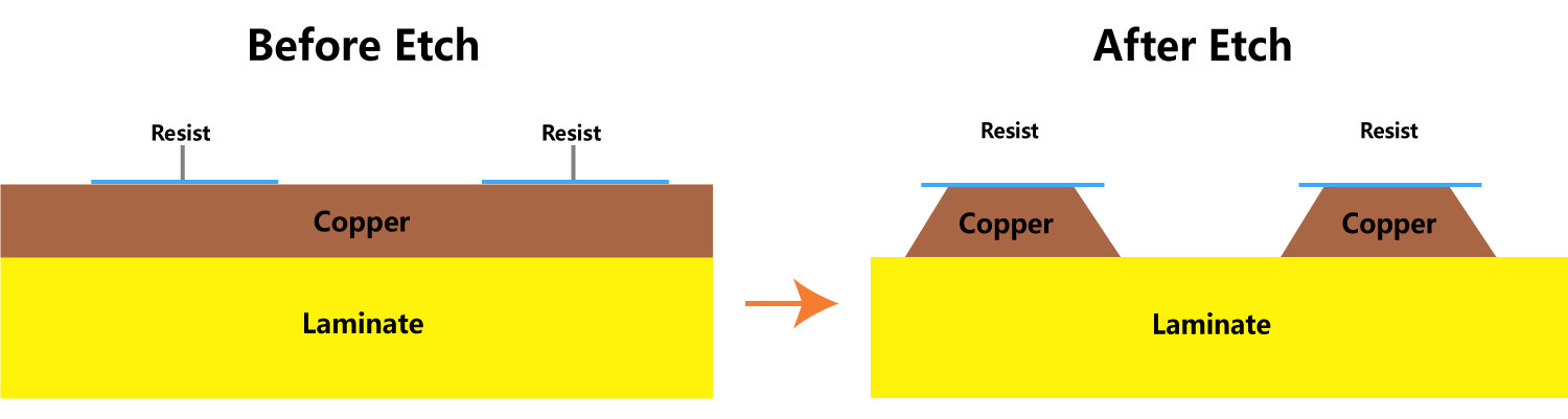
When the chemicals trim down the copper excesses toward the laminate, they laterally trim the coppers under the resist, resulting in a trapezoidal shape to copper features. This etching takes time, and the thicker your Copper PCB, the more time-consuming it becomes.
Additionally, suppose the film elements are too close to each other. In that case, it won’t be easy to etch down to the laminate, reducing the copper features and ruining the PCB design completely.
Conclusion
Copper thickness is an integral part of Printed Circuit Board designs. It helps save time and allows the proper spacing between copper features to improve workability. The standard thickness for Copper PCBs is 1 oz (1.38 mils).
Ensure you note your copper thickness parameters to your PCB manufacturer to ensure your designs are true to life. If you want to design a thicker Copper PCB, note that it becomes expensive, and the time required to plate and etch properly will increase.
At NextPCB, we take copper thickness seriously. While many PCB designs are custom-made and tailored to serve the consumer's needs, many do not specify the thickness of their circuit boards. Hence, at NextPCB, we tend to go with the standard thickness of copper-printed circuit boards- 1 oz.
It is our top priority to ensure we deliver quality PCB designs to your doorstep. Contact us for more information regarding 1 oz copper PCB and enjoy our impressive customer service.