- PCB Specifications
-
Items: Layer count
Manufacturing Capabilities: 1 - 32 layers
Notes:Quantity of copper layers on the board
Items: Impedance
Manufacturing Capabilities: For 4, 6, 8, 10, 12, 14, 16, 18, 20 layers PCB, PCB Stackup designed by NextPCB(by default), or PCB Stackup designed by customers
Notes: Layer Stackup Structure Impedance Calculation Parameter
Items: Impedance tolerance
Manufacturing Capabilities: ±10%
Items: Material
Manufacturing Capabilities: FR-4
Notes: FR-4: TG130/TG150/TG170
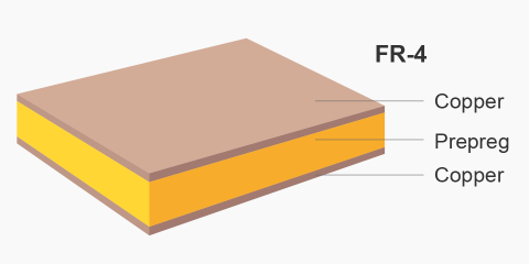
Items: PCB material dielectric constant
Manufacturing Capabilities: 4.2
Notes: Prepreg dielectric constant (prepregtype: 7628/1080/2313/2116, dielectric constant: 4.2)
Items: Max. dimension
Manufacturing Capabilities: 1-2 layers: 500*600mm 4-20 layers: 400*500mm
Notes: The maximum dimension that NextPCB can do
Items: Min. dimension
Manufacturing Capabilities: Length and width ≥10mm
Notes: Min. dimension = 10*10mm
Items: Dimension tolerance
Manufacturing Capabilities: CNC: ±0.15mm, V-CUT: ±0.2mm
Notes: ±0.15mm for CNC routing,and ±0.2mm for V-scoring
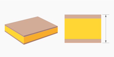
Items: PCB thickness
Manufacturing Capabilities: 0.6/0.8/1.0/1.2/1.6/2.0/2.5/3.0/3.2mm
Notes: The thickness of finished board
Items: Thickness tolerance( Thickness≥1.0mm)
Manufacturing Capabilities: ±10%
Notes: e.g. If the board thickness is 1.6mm, the finished board thickness ranges from 1.44mm(1.6-1.6×10%) to 1.76mm(1.6+1.6×10%)
Items: Thickness tolerance( Thickness < 1.0mm)
Manufacturing Capabilities: ±0.1mm
Notes: e.g. If the board thickness is 0.8mm, the finished board thickness ranges from 0.7mm(0.8-0.1) to 0.9mm(0.8+0.1)
Items: Finished copper weight
Manufacturing Capabilities: 1 oz/2 oz
Notes: Finished copper weight of outer layer could be 1 oz/2 oz
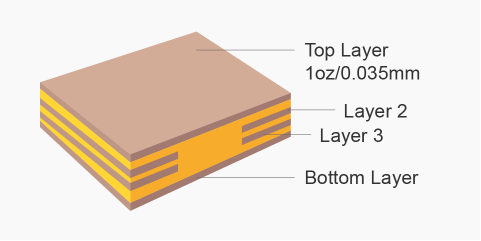
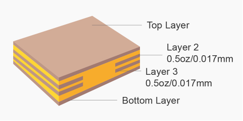
Items: Inner copper weight
Manufacturing Capabilities: 0.5 oz/1 oz/2 oz
Notes: Finished copper weight of inner layer could be 0.5 oz/1 oz/2 oz
Items: Surface finish
Manufacturing Capabilities: HASL/Lead free HASL/ENIG/OSP
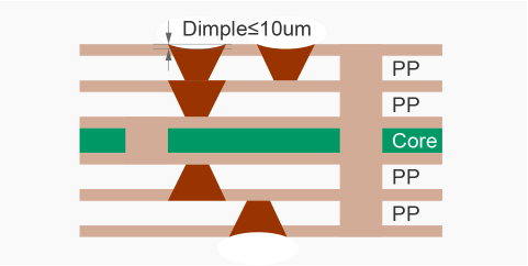
Items: HDI structure
Manufacturing Capabilities: Type 1 /Type 2 /Type 3
Notes: Mechanical blind buried vias or laser blind buried vias(electroplating Via-filling is available) or laser blind vias filling dimple ≤ 15µm
Items: Electrical test
Manufacturing Capabilities: Flying Probe/Special test fixture
Notes: No limits for Flying Probe. Max. 14000 Pads can be tested by PCB test fixture
Items: Beveling angle of gold finger
Manufacturing Capabilities: 20°/30°/45°/60°
Items: Beveling angle tolerance of gold finger
Manufacturing Capabilities: ±5°
Items: Beveling depth tolerance of gold finger
Manufacturing Capabilities: ±0.1mm
Items: Outline tolerance
Manufacturing Capabilities: ±0.15mm
Items: V-CUT angle
Manufacturing Capabilities: 30°/45°/60°
Items: Number of V-CUT
Manufacturing Capabilities: ≤30 cuts
Items: V-CUT outline size
Manufacturing Capabilities: 55mm ≤ length/width ≤ 480mm
Items: V-CUT residue thickness
Manufacturing Capabilities: 0.25mm ≤ v-cut residue thickness ≤ 0.4mm
- Drill/Hole Size
-
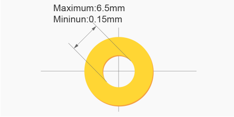
Items: Drill hole size(Mechanical)
Manufacturing Capabilities: 0.15-6.5mm
Notes: Min. drill hole size: 0.15mm(available for PCB thickness ≤ 1.2mm) Max. diameter of drilling bits is 6.5mm(contact support@nextpcb.com if your customed hole size > 6.5mm)
Items: Drill hole size tolerance
Manufacturing Capabilities: ≤0.05mm
Items: Blind/Buried vias
Manufacturing Capabilities: Mechanical blind buried vias: copper thickness of blind vias ≥ 20µm
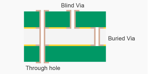
Items: Blind/Buried vias
Manufacturing Capabilities: Laser blind buried vias: dimple ≤ 10µm
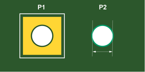
Items: Via pad size
Manufacturing Capabilities: ≥0.1
Notes: The pad hole size will be enlarged 0.125mm in production
Items: PTH hole size
Manufacturing Capabilities: 0.2mm (for single side)
Notes: The annular ring size will be enlarged to 0.2mm in production
Items: Min. non-plated holes
Manufacturing Capabilities: 0.4mm
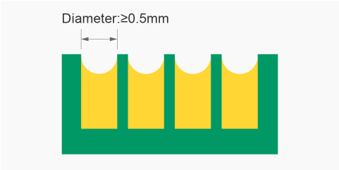
Items: Min. plated slots
Manufacturing Capabilities: 0.5mm

Items: Min. non-plated slots
Manufacturing Capabilities: 0.5mm
Items: Min. castellated holes
Manufacturing Capabilities: 0.5mm
Notes: The minimum diameter of castellated holes is 0.50mm
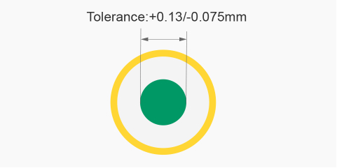
Items: Hole size tolerance(Plated)
Manufacturing Capabilities: ±0.075mm
Notes: e.g. If customed Plated hole size is 1.000mm, the finished hole size could be between 0.925mm to 1.075mm
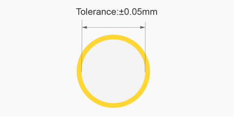
Items: Hole size Tolerance(Non-Plated)
Manufacturing Capabilities: ±0.05mm
Notes: e.g. If customed Non-Plated hole size is 1.000mm, the finished hole size could be between 0.95mm to 1.05mm
Items: Rectangle hole/Slot
Manufacturing Capabilities: With or without fillet angle

- Minimum Annular Ring
-
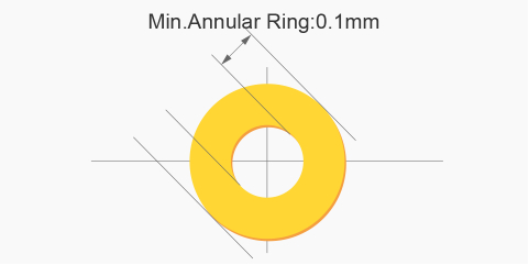
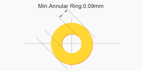
Items: 1 oz Copper
Manufacturing Capabilities: 3.5mil (single side) (3.5mil≈0.09mm)

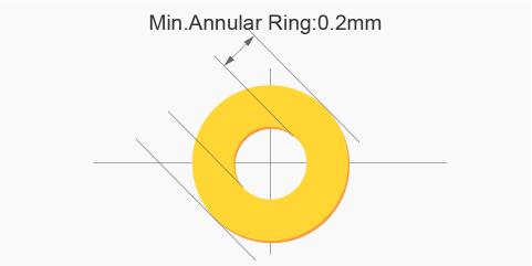
Items: 2 oz Copper
Manufacturing Capabilities: 4.5mil (single side) (4.5mil≈0.11mm)
- Minimum clearance
-
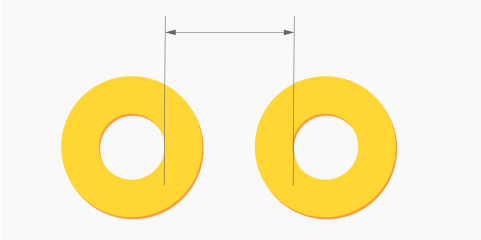
Items: Hole to hole clearance(Different nets)
Manufacturing Capabilities: ≥12mil(Avoid conductive anodic filament)(12mil≈0.30mm)
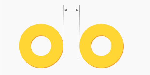
Items: Via to via clearance(Same nets)
Manufacturing Capabilities: ≥8mil (8mil≈0.20mm)

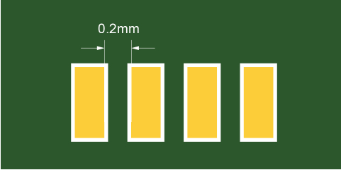
Items: SMD pad to SMD pad clearance(Pad without hole, different nets)
Manufacturing Capabilities: ≥0.15mm
Items: Pad to pad clearance(Pad with hole, different nets)
Manufacturing Capabilities: ≥0.40mm
Items: Via to track
Manufacturing Capabilities: ≥7mil (7mil≈0.18mm)
Items: PTH to track
Manufacturing Capabilities: ≥9mil (9mil≈0.23mm)

Items: NPTH to track
Manufacturing Capabilities: ≥8mil (8mil≈0.20mm)

Items: SMD pad to track
Manufacturing Capabilities: ≥4mil (4mil≈0.10mm)
- Minimum trace width and spacing
-
Copper weight: H/HOZ(0.5oz Inner layer)
Min. trace width: 2.5mil (2.5mil≈0.06mm)
Min. spacing: 3mil (3mil≈0.08mm)
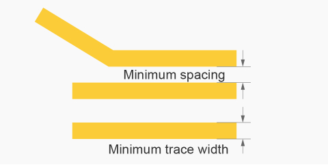
Copper weight: 1 oz(Outer layer)
Min. trace width: 3mil (3mil≈0.08mm)
Min. spacing: 3mil (3mil≈0.08mm)

Copper weight: 2 oz(Outer layer)
Min. trace width: 5.5mil (5.5mil≈0.14mm)
Min. spacing: 5.5mil (5.5mil≈0.14mm)

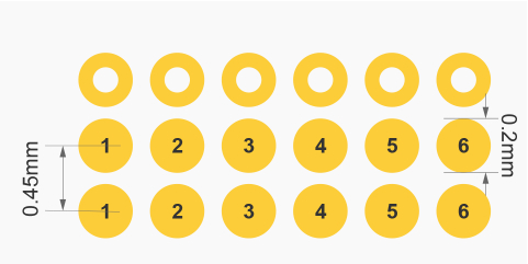
- BGA
-
Layer count: 1 oz
Min. BGA pad dimensions: ≥0.2mm
Min. distance between BGA: 0.15mm
Min. spacing between the center of two BGAs: 0.45mm
- Solder Mask
-
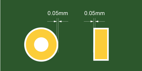
Items: Solder mask opening/expansion
Manufacturing Capabilities: ≥1.5mil (1.5mil≈0.04mm)
Notes: There should be a minimum size of 1.5mil "solder mask opening" around the pad to allow for any misregistration
Items: Solder bridge
Manufacturing Capabilities: Green: 3.5mil Black/White: 5mil other solder mask: 4mil
Notes: To build solder bridge, the spacing between copper pads edge must be 3.5mils or more
Items: Solder mask color
Manufacturing Capabilities: Green/Red/Yellow/Blue/White/ Matte Black/Black
Items: Solder mask dielectric constant
Manufacturing Capabilities: 3.5
Items: Solder mask thickness
Manufacturing Capabilities: Solder mask thickness on base material: 0.8mil, solder mask thickness on copper: 0.6mil
- Legend
-
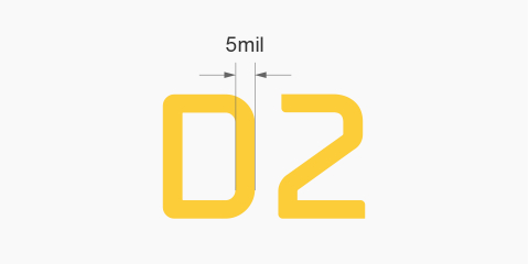
Items: Minimum line width
Manufacturing Capabilities: Silkscreen printing≥5mil (5mil≈0.12mm) Printer printing≥3mil (3mil≈0.08mm)
Notes: Characters width < 3mil(0.076mm) will be unidentifiable
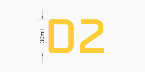
Items: Minimum text height
Manufacturing Capabilities: Silkscreen printing≥30mil (30mil≈0.76mm) Printer printing≥24mil (24mil≈0.61mm)
Notes: Characters height < 24mil(0.61mm) will be unidentifiable
Items: Character width to height ratio
Manufacturing Capabilities: ≥ 6:1
Notes: The preferred ratio of width to height is 6:1
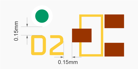
Items: Pad to silkscreen
Manufacturing Capabilities: >6mil (6mil≈0.15mm)
Notes: The minimum distance between pad and silkscreen is 0.15mm
- Board Outlines
-
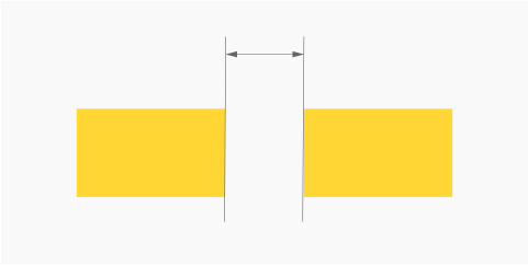
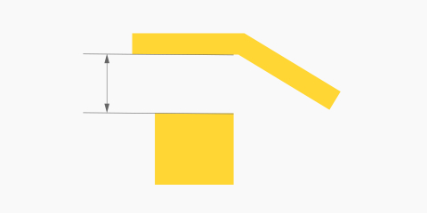
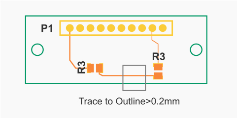
Items: Trace to outline
Manufacturing Capabilities: ≥0.2mm
Notes: Individual board(Rounting): Trace to Outline ≥ 0.2mm
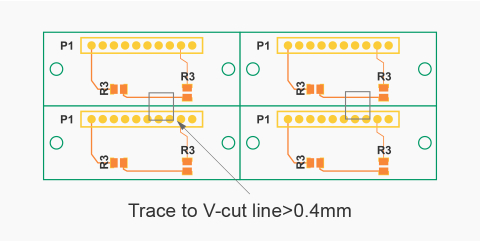
Items: Trace to V-cut line
Manufacturing Capabilities: ≥0.4mm
Notes: Panel board with V-scoring: Trace to V-cut line ≥0.4mm
- Panelization
-
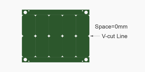
Items: Panelization without space
Manufacturing Capabilities: 0mm
Notes: No space between panelized PCBs
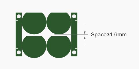
Items: Panelization with space
Manufacturing Capabilities: ≥1.6mm
Notes: The space between panelized PCBs should ≥ 1.6mm, if not, the routing process may be difficult and low efficiency
Items: Panelized round board
Manufacturing Capabilities: ≥80mmx80mm
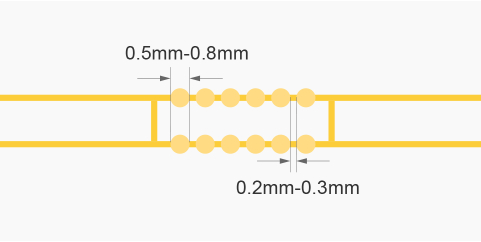
Notes: Stamp Hole: hole size=0.5mm, copper gap=0.35mm, 5-7holes for a set by default
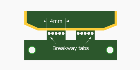
Items: Panelized castellated holes board
Manufacturing Capabilities: Panelize with stamp holes and add tooling strips on four board edges
Notes: The distance between castellated hole and board corner should be > 4mm
Recommended diameter of stamp hole is 0.5mm-0.8mm
Recommended distance between the two stamp holes is 0.2mm-0.3mm
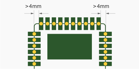
Items: Min. width of breakaway tab
Manufacturing Capabilities: ≥4mm
Notes: The minimum width of breakaway tab is 4mm. For breakaway with mouse-bites, the minimum width is 5mm
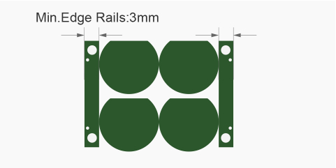
Items: Min. edge rails
Manufacturing Capabilities: ≥3mm
Notes: If you choose panel by NextPCB, we will add 3mm edge rails on both sides by default
- Manufacturable Notes for Different PCB Design Softwares
-
Items: PADS
Manufacturing Capabilities: copper-pour pattern
Notes: NextPCB Fab uses hatch pattern by default, please note your copper-pour pattern when placing an order
Items: PADS
Manufacturing Capabilities: 2D line
Notes: Valid lines cannot be placed in the corresponding layer as 2D lines, NextPCB does not process 2D lines
Items: Altium Designer Protel
Manufacturing Capabilities: Version
Notes: There are elements missing issues in generating Gerber files from different versions of Altium Designer. Please note your version No. of Altium Designer when placing an order
Items: Altium Designer Protel
Manufacturing Capabilities: Parts outside PCB
Notes: If the components were placed far away from the PCB board, file generating would failed because the boundary of the board is too large
Items: Altium Designer Protel
Manufacturing Capabilities: solder mask opening
Notes: Please do not put the opening of the solder layer on the paste layer by mistake, NextPCB does nothing to the paste layer
Items: Altium Designer Protel
Manufacturing Capabilities: copper-pour pattern
Notes: Fill pattern: too much filling region will causing region missing when generating a file, Tip: choosing Polygon copper-pour pattern