-
-
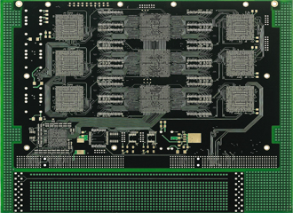
Blind & Buried Via PCB
Material: FR4 Tg180
PCB Thickness: 2.0mm
Min. Trace / Space Outer: 0.127mm/0.127mm
Min. Drilled Hole: 0.25mm
Surface Finish: ENIG
Product Features
NextPCB HDI PCB Manufacturing Capabilities
NextPCB specilizes in reliable multilayer PCB manufacture including HDI PCBs up to HDI Class 3, and any layer PCBs with the Advanced PCB service for prototype, small batch and mass production requirements. See the table below for a snapshot of our capabilities and services.
| Specification | Capability |
|---|---|
| HDI Structures | HDI Class I, II, III, (any layer HDI Advanced PCB) |
| Standard HDI Stack-ups | 1+n+1, 2+n+2, 3+n+3 |
| Materials | High-TG, High-Speed, High-Frequency laminates and more |
| Vias | Microvias, blind/buried vias, filled and plated vias/via-in-pad (POVF) |
| Min. Laser Via Diameter | 0.075 - 0.15mm |
| Max. Laser Via Aspect Ratio | 1:1 (0.75:1 recommended) |
| Max. Filled Via Diameter | 0.45mm |
| Blind Via Dimple | ≤10um |
| Min. Trace Width/Spacing | 3.5/3.5 mil (2/2 mil Advanced PCB) |
| Min. Pad Size | 8 mil |