BGA Assembly Capabilities
Ball Grid Array PCB Manufacturing: Design, Process & Quality Control
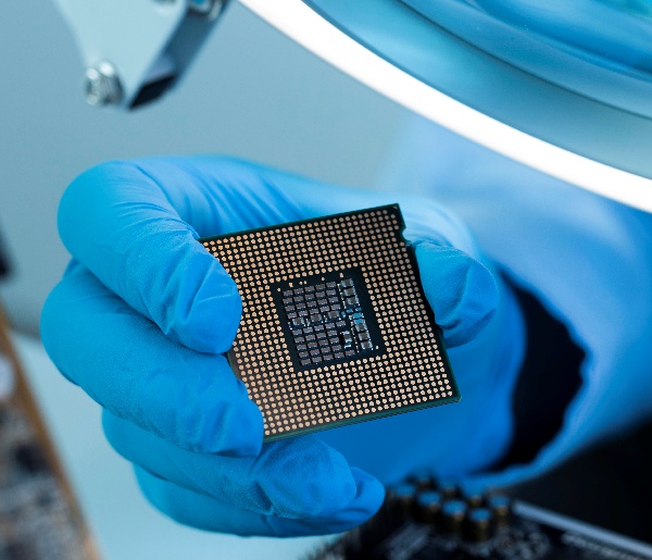
Ball Grid Array (BGA) technology revolutionized electronics manufacturing by enabling the dense, high-performance devices powering our world. At NextPCB, we've refined BGA assembly to deliver unparalleled reliability in complex applications – from micro-BGAs in wearables to large ceramic BGAs in aerospace. Here's your comprehensive roadmap to mastering this critical process.
BGA Fundamentals: What Is BGA Assembly and Why It Matters?
Core Principle:
BGAs replace fragile leads with solder ball arrays underneath the package. This design delivers:
- 30-50% higher I/O density vs. QFP
- Shorter signal paths → superior high-speed performance
- Reduced inductance (critical for RF/CPU designs)
- Enhanced thermal dissipation through direct PCB connection
Top 9 Most Common IC Packaging Types in Modern Electronics
Types of BGA Packages (P-BGA, F-BGA, C-BGA, T-BGA)
(Per IPC-7095E Standards)
|
Type |
Name |
Key Properties |
Best Applications |
|
P-BGA |
Plastic BGA |
Cost-effective, moisture-sensitive |
Consumer devices, routers |
|
F-BGA |
Flip-Chip BGA |
Ultra-thin profile, fine pitch (<0.5mm) |
Smartphones, micro-BGA packages |
|
C-BGA |
Ceramic BGA |
Extreme thermal/mechanical resilience |
Automotive, aerospace |
|
T-BGA |
Tape BGA |
Flexible interconnects |
Medical sensors, wearables |
Critical Assembly Challenges:
1. Hidden Joints: 100% X-ray
2. Moisture Sensitivity: MSL 2-3 components require:
- Dry storage (<5% RH)
- 24hr baking (125°C) before assembly
3. CTE Mismatch: Dynamic warpage during reflow → non-wet opens/cracks
4. Stress Fractures: Corner balls fail first → avoid placement near:
- Board edges
- Mounting screws
- Flex points
BGA Assembly Process: Step-by-Step Breakdown
Stage 1: PCB and Component Preparation
PCB Treatment:
- ENIG surface finish (ideal for µBGAs)
- Laser-microvias (≤100μm) for HDI boards
- Solder mask-defined (SMD) pads for pitch <0.4mm
Component Prep:
- Bake per JEDEC J-STD-033
- Pre-heating (80-100°C) to minimize thermal shock
Stage 2: Solder Paste Selection and Stencil Design
|
Parameter |
Standard BGA |
Micro-BGA |
|
Solder Paste |
Type 4 (20-25μm) |
Type 5 (10-15μm) |
|
Stencil Ratio |
1:1 |
0.85:1 (Nano-coated) |
|
Placement Accuracy |
±30μm |
±15μm |
|
Vision System |
2D Alignment |
3D Laser Scanning |
Stage 3: Post-Reflow Inspection: AOI, AXI, Boundary Scan
1. AOI: Checks coplanarity (±50μm) and misalignment
2. AXI: Detects:
- ≥5% voids (critical for power BGAs)
- Head-in-Pillow defects
- Micro-cracks
3. Boundary Scan: Electrical validation
4. Acoustic Microscopy: Delamination analysis
Common BGA Failure Modes and How to Prevent Them
|
Failure Mode |
Detection Method |
Prevention Strategy |
|
Non-Wet Opens (NWO) |
Cross-section SEM |
Optimize flux activity temperature |
|
Solder Ball Cracks |
Dye-and-Pry Test |
Corner underfill application |
|
Pad Cratering |
TDR Testing |
Low-CTE PCB materials |
|
Popcorning (MSD) |
CSAM (C-Mode Scanning) |
Strict moisture floor life control |
7 Competitive Advantages of BGA Assembly
- 70% Size Reduction: Integrates Xilinx FPGAs into IoT modules
- 60% Weight Savings: Critical for medical implants
- >99% First-Pass Yield: With optimized stenciling
- 40°C/W Lower θJA: Thermal performance benchmarks
- 5G-Signal Integrity: <0.1dB insertion loss at 28GHz
- Shock Resistance: 1500G survivability vs. 500G for QFNs
- Automated Rework: BGA belt guard assembly C715 compatible
Future-Proofing Your Designs
NextPCB's Roadmap for Next-Gen BGA Solutions:
- Ultra-Fine Pitch: 0.2mm µBGAs for neural implants
- Hybrid Bonding: Cu-Cu interconnects for 3D packages
- Low-Temp Solder: Sn-Bi alloys for flexible substrates
- ML-Driven X-ray: Real-time void prediction (patent-pending)
- Active Alignment: MEMS-based component placement
Your Turnkey BGA Assembly Solution
- NextPCB delivers certified IPC-7095E processes for:
- Prototype to Volume: 48-hour turnaround for BGA pcb assembly quotes
- µBGA Expertise: 01005 component capability
- Full Testing: Including 3D X-ray tomography
- Complex Projects: Soldered cold plate bga assembly process
Get Real-Time Pricing: Click for Instant BGA Online Assembly Quote
FAQs: BGA Assembly Essentials — NextPCB FAQ
Q1: How accurate are NextPCB's online BGA assembly quotes?
Our online quoting system factors in real-time material costs, IPC class specifications, and project complexity. Most quotes are highly accurate and remain valid for 30 days. For projects involving complex layouts or special process requirements, we recommend consulting our engineering team to confirm final pricing.
Q2: What's the minimum BGA pitch NextPCB supports?
We support BGA packages with a minimum pitch of 0.25 mm, including 100% X-ray inspection for all BGA solder joints. If your design requires finer pitch (e.g., 0.20 mm), please contact our engineering team for feasibility assessment.
Q3: Can you repair cracked BGA solder joints caused by thermal cycling?
Yes. We provide professional BGA rework services using precision rework stations and X-ray verification. If your repair process requires underfill injection or Scanning Acoustic Microscopy (SAM), please consult us to evaluate custom solutions.
Q4: How does BGA vs QFN assembly affect signal integrity?
BGA packages offer significantly lower parasitic inductance (<0.1 nH), making them ideal for RF and high-speed digital applications above 800 MHz. QFN packages are more suitable for simpler designs where visual inspection and lower cost are priorities. For GHz-level performance, we generally recommend BGA.
Q5: What level of IPC-7095E compliance do you offer for BGA assembly?
We support full IPC-7095E Class 3 assembly standards upon request, including 100% X-ray inspection, void control, and traceability under ISO 9001 quality management. If you require specific voiding thresholds (e.g., ≤5%), please indicate this in your RFQ for confirmation.
Q6: Can you integrate soldered cold plates in BGA assemblies with thermal resistance ≤0.15 °C/W?
At present, soldered cold-plate integration is not part of our standard service offering. If your project requires integrated thermal management (e.g., bonded copper plates, thermal interface materials), please provide detailed mechanical and thermal specifications for evaluation.
You may also interested in: